
Simulation and Design
CHFE maintains software such ANSYS EM packages for high-frequency electromagnetic field simulation, Keysight Advanced Design System (ADS) for RF electronics design, IC-CAP for DC and RF semiconductor device modeling, and Microwave Office for designing all types of RF and microwave circuits.
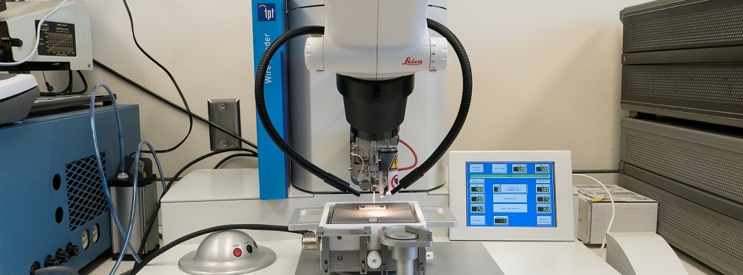
PCB Fabrication and Back-end Processing
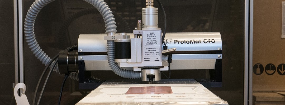
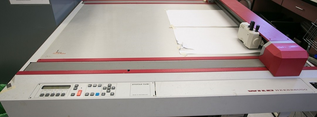
CHFE has equipment including PCB mask plotter, PCB reflow oven, rework station, UV lithography tool, wet etching bench, LPKF milling machine, dicing saw (Disco DAD321), wire bonder (TPT HB16) and wedge bonder (Westbond) for wedge/ball wire bonding (wire/ribbon, Al/Au).
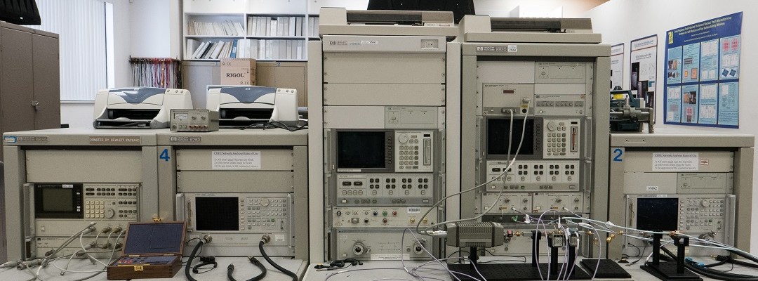
Characterization and Measurement
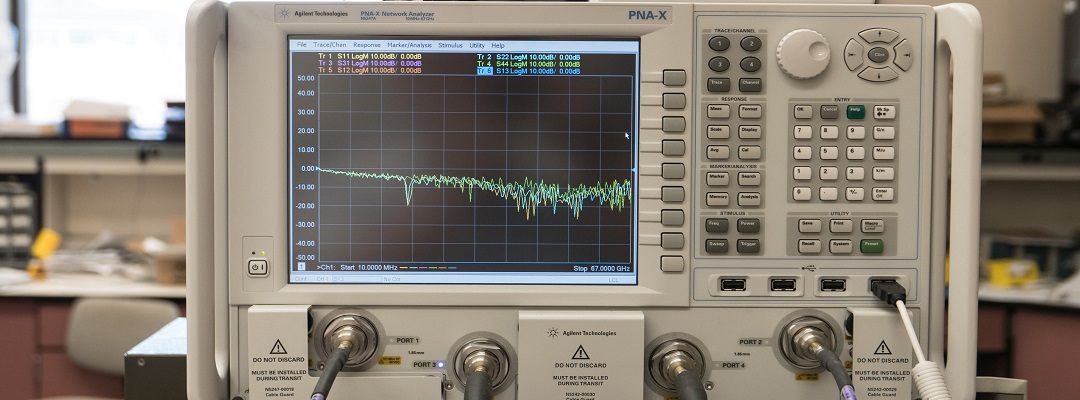
CHFE supports microwave and millimeter wave devices characterization with equipment such as Agilent N5247A PNA-X vector network analyzer, Cascade SUMMIT 9300 RF probe station, synthesized sweepers, spectrum analyzers and oscilloscopes.
Integrated NanoMaterials Laboratory
The Integrated Nanomaterials Laboratory (INML) is a state-of-the-art nanomaterials synthesis and characterization facility. INML addresses the critical technological needs of the future through material development as we integrate nanoscience with disciplines such as electronics, photonics, renewable energy, chemistry, biology, and physics.